Electrostatic chuck is a key component widely used in semiconductor manufacturing for clamping and positioning semiconductor chips. In the past, China's semiconductor industry relied mainly on imports for electrostatic chucks, which brought great inconvenience to domestic semiconductor manufacturing.
In view of international trade friction and technology protection pressure, China decided to increase the localization of electrostatic chucks. However, to achieve this goal is not easy, facing a series of technical and market difficulties.

Technical breakthroughs in the arduous
As a high-precision component, electrostatic chucks require extremely low coefficient of friction, stable mechanical properties and high-precision positioning capability. In order to realize localization, Chinese semiconductor enterprises actively carry out technical research.
After years of efforts, domestic enterprises have made some breakthroughs. They have improved the process, optimized the material ratios, and developed some innovative design methods. These technological advances have significantly improved the performance of domestic electrostatic chucks.
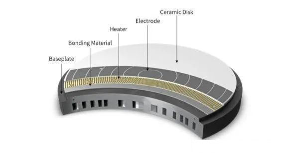
Structure of electrostatic chuck
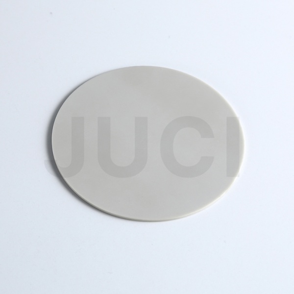
Conventional electrostatic chuck, the difference is that the surface of the electrostatic chuck insulation layer material is different, dark aluminum nitride, white alumina, the structure of the electrostatic chuck is divided into the following parts:
- Insulation layer: Used for contact with wafers, usually aluminum nitride ceramic, because of its good mechanical strength, high temperature resistance and thermal conductivity.
- Ejector pin and He air holes: The ejector pin is used for wafer transfer. When the wafer enters the etching chamber, the ejector pin rises to take up the wafer, and then the ejector pin falls down to place the wafer on the surface of the electrostatic chuck. Moreover, the ejector is usually a hollow structure, and He gas is passed through to cool down the wafers at the same time.
- Back He flow: Used to enhance heat dissipation and to provide feedback on wafer adsorption.
- Electrostatic Electrodes: Used to generate an electrostatic field to adsorb wafers. Electrodes are usually flat and embedded or deposited in insulating materials. Commonly used materials include aluminum, copper and tungsten and other metals with good electrical conductivity.
- Circulating cooling water and heating electrodes: mainly used for the overall temperature control of the electrostatic chuck, heating electrodes and circulating cooling water at the same time, so that the wafer can be maintained at a stable temperature.

The key and difficult point of the electrostatic chuck lies in the temperature control.
Semiconductor process temperature control of the wafer is critical to dry etching, for example, the need to control the wafer at 100 ° C to -70 ° C at a particular temperature to maintain a certain etching characteristics, and therefore the need for static chuck on the wafer to heat or heat dissipation, so as to accurately control the wafer temperature.
With the development of a new generation of semiconductor technology, low-temperature etching and deposition processes usually require wafers to reach lower temperatures, so the heat dissipation performance of the electrostatic chuck has put forward higher requirements.
From a technical point of view, in addition to the size of the wafers carried by the gradual increase in size, the development trend of electrostatic chuck is mainly manifested in the temperature uniformity control needs to improve, that is, the number of zoned temperature-controlled temperature zones gradually increased.
Before and after 2000, the number of zoned temperature control temperature zone is generally 2 zones, 2000 to 2005, the number of zoned temperature control temperature zone is generally 4 zones, and at this stage, there are more than 100 temperature zone of the electrostatic chuck products have been developed and put into practical applications.
The bright future of domestic electrostatic chuck
Although the road to localization faces difficulties and challenges, but the domestic semiconductor enterprises in the localization of electrostatic chuck has made remarkable progress. With the continuous maturation of technology and brand enhancement, the market share of domestic electrostatic chucks is gradually increasing. And, China as the world's largest semiconductor market, the demand for electrostatic chucks will continue to grow.
The localization of electrostatic chucks is an important part of China's semiconductor industry to achieve self-control. Although facing technical breakthroughs and market competition in the arduous, but China's semiconductor enterprises are actively promoting the localization of electrostatic chuck process. It is believed that with the passage of time, the domestic electrostatic chuck will be more mature and show strong competitiveness in the market.

About Xiamen Juci Technology Co., Ltd.
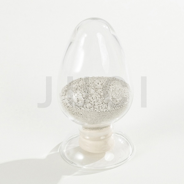
Xiamen Juci Technology Co., Ltd. is a cutting-edge high-tech enterprise dedicated to the R&D, manufacturing, and distribution of premium aluminum nitride (AlN) materials. As an industry-leading AlN powder producer, we deliver high-performance material solutions tailored for advanced applications in electronics, semiconductor, and aerospace sectors. Our commitment to excellence in product quality and customer service has established us as a trusted global partner for specialized ceramic materials.
Media Contact:
Xiamen Juci Technology Co., Ltd.
Phone: +86 592 7080230
Email: miki_huang@chinajuci.com
Website: www.jucialnglobal.com